Intel has revealed some interesting details about their upcoming Lakefield SOC which utilizes the Foveros 3D packaging technology. The new SOC will be the first from Intel utilizing 3D integration that will allow for much smaller chip packages which would help create a range of new platforms and PC form factors.
Intel Lakefield SOC with Foveros 3D Packaging Previewed – 10nm Hybrid CPU Architecture, Gen 11 Graphics, Multiple Dies Stacked on Top of Each Other
Intel Lakefield is based around Foveros technology which helps connect chips and chiplets in a single package that matches the functionality and performance of a monolithic SOC. Each die is then stacked using FTF Micro-bumps on the active interposer through which TSVs are drilled to connect with solder bumps and eventually the final package. The whole SOC is just 12×12 (mm) which is 144mm2.
Related Intel GPU “Iris Plus Graphics 940” With Gen 11 Graphics Architecture Early Benchmarks Leak Out – Hugely Improved Over Existing Intel iGPUs, Beats Out Vega 11 Graphics
At CES 2019, Intel previewed a new client platform, code-named “Lakefield,” featuring the first iteration of its new innovative Foveros 3D packaging technology. This hybrid CPU architecture enables combining different pieces of IP that might have previously been discrete into a single product with a smaller motherboard footprint, which allows OEMs more flexibility for thin and light form factor design. Lakefield is expected to be in production this year.
(Credit: Intel Corporation)

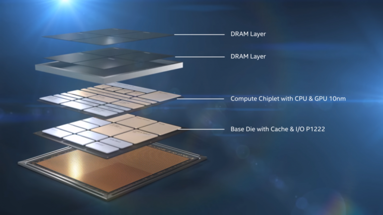
Talking about the SOC itself and its individual layers, the Lakefield SOC that has been previewed consist of at least four layers or dies, each serving a different purpose. The top two layers are composed of the DRAM which will supplement the processor as the main system memory. This is done through the PoP (Package on Package) memory layout which stacks two BGA DRAMs on top of each other as illustrated in the preview video. The SOC won’t have to rely on socketed DRAM in this case which saves a lot of footprint on the main board.
The second layer is the Compute Chiplet with a Hybrid CPU architecture and graphics, based on the 10nm process node. The Hybrid CPU architecture has a total of five individual Cores, one of them is labeled as the Big Core which features the Sunny Cove architecture. That’s the same CPU architecture that will be featured on Intel’s upcoming 10nm Ice Lake processors. The Sunny Cove Core is optimized for high-performance throughput. There are also four small CPUs that are based on the 10nm process but optimized for power efficiency.
The same die consists of Intel’s Gen 11 graphics engine with 64 Execution Units. Last week, we got to see the performance of an Intel GT2 (Gen 11) Iris Plus 940 graphics chip with 64 Execution Units and the results were quite good compared to existing Intel Gen 9.5 graphics chips. You can check out the performance results here.
Knowing that the Lakefield SOC will feature the same graphics engine, we can expect a very decent graphics performance out of this 3D stacked processor. Then last of all is the base die which serves as the cache and I/O block of the SOC. Labeled as the P1222 and based on a 22FFL process node, the base die comes with a low cost and low leakage design while providing a feature-rich array of I/O capabilities.
Given the extremely tiny chip size and the resultant smaller board sizes, Intel expects Forveros and Lakefield would unleash a wave of new, uncompromised, PC devices, platforms and a range of an entirely new class of devices in the coming years. Surely, Lakefield SOCs will be the first 3D design for a compute heavy and power efficient SOC and we would really like Intel to share some power and performance numbers of their upcoming SOC which is expected to go in production this year.


