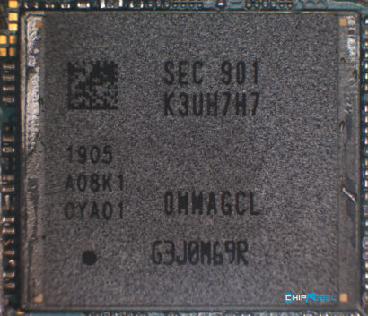
As the days pass after Samsung’s Galaxy S10 launch, we’re starting to see in-depth information for the gadgets’ performance come to light. Samsung’s launched the three smartphones with a host of new technologies, that also cover their display and processor. The Galaxy S10 lineup, like Samsung’s other premium mobile gadgets, are powered by different processors in different regions. Its international and South Korean variants run on Samsung’s Exynos 9820, which is manufactured on the company’s in-house 8nm process.
Today, the good folks over at Chip Rebel have taken the Exynos 9820 apart and snapped a couple of photographs. Interested? Head over below for more details.
Related Samsung Galaxy S10’s Facial Recognition Easily Fooled by a Digital Image
Die Shot Of Samsung’s Exynos 9820 Shows A Larger Surface Area Than Its Predecessor; Samsung’s Custom SoC Loses Out To Apple, Qualcomm In Area
Over the past couple of years, Samsung’s processors haven’t been what they used to. At one time in the past, the Korean tech was able to give Qualcomm touch competition in overall computing performance, and its SoCs only lost out to the Snapdragon lineup in graphics performance. But now, the Exynos isn’t in the same league as the San Diego chip giant’s high-end silicon, and the Exynos 9810 with its cache problems only augmented the performance decline.
With the Exynos 9820, Samsung made some important changes to the lineup’s architecture. Like Qualcomm’s Snapdragon 855, the Korean tech giant freed up die space by replacing two of earlier designs’ larger cores with two middle sized ones. This changed the core configuration to 2+2+4, from 4+4 found on earlier designs. Now that Chip Rebel’s die shots are out, we can take a look at how these changes appear in the flesh.
As you can see in the final image above, CPU configuration for the Exynos 9820 is different from that of its predecessor. The Exynos 9820 had problems with cache access, and to rectify these, Huawei has added an additional L3 cache to connect the Cortex A75 and Cortex A55 cores. Additionally, owing to their heavy workload requirements, the two ‘big’ custom Mongoose M4 cores get an L3 cache of their own. Samsung’s chip also fails to impress in surface area, as it occupies a space of 127mm², which is greater than any other comparable processor’s right now. Apple’s A12, manufactured by TSMC, has a die surface area of 83.27mm².
Take a look at the right side of the of the colored die shot and you’ll also see the 12 core Mali GPU that powers the Exynos 9820. Additionally, anyone who’s interested in a ‘Neural Engine’ can also be assured that physically (i.e. on silicon), a neural engine is virtually indistinguishable from a GPU. What separates them is the type of tasks that the cores are programmed to handle. With these details, let’s take a look at how Samsung’s Exynos 9820 and Huawei’s Kirin 980 look like.
Starting off with the Kirin 980 (identification courtesy Anandtech) we can see that the layout of the high-performance and low-performance cores on the Kirin 980 is different than that found on the Exynos 9820. Additionally, while Samsung’s processor uses two L3 representations, Huawei’s processor uses the same silicon for all the cores. The Exynos 9810, owing to its different cluster architecture dedicates more area to the performance intensive big cores.
Thoughts? Let us know what you think in the comments section below and stay tuned. We’ll keep you updated on the latest.
Products mentioned in this post


